Il Fe ha verniciato GaN Substrates Resistivity > 10 ⁶ Ω·Dispositivi di cm rf
Prezzo: Negotiable
MOQ: Negotiable
Tempo di consegna: 3-4 week days
Marca: GaNova
Evidenziare:ISO GaN Substrates, gan semiconductor wafer, Fe Doped GaN Substrates
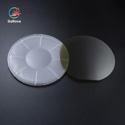
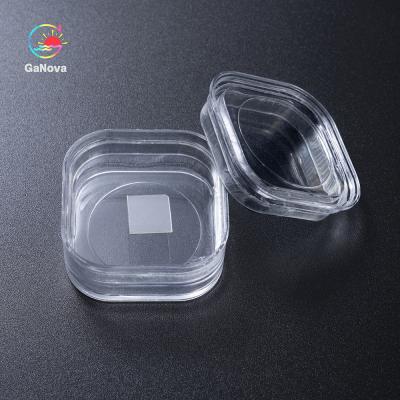
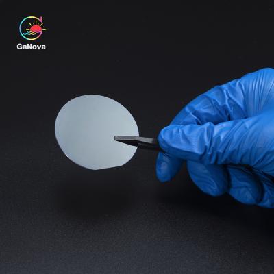
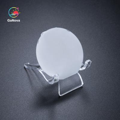
2inch C-face Fe-doped SI-type free-standing GaN single crystal substrate Resistivity > 106 Ω·cm RF devices The achieved breakdown voltage of the Fe-doped GaN epitaxial layer can be as high as 2457 V, which is attributed to the Fe-doped GaN epitaxial layer with higher resistance, which can sustain... Visualizza di più
Contatta ora
4 pollici 4H-SiC Substrato P-livello SI 500.0±25.0μm MPD≤5/cm2 Resistenza≥1E5Ω·cm
Prezzo: Negotiable
MOQ: Negotiable
Tempo di consegna: 3-4 week days
Marca: GaNova
Evidenziare:Substrato 4H-SiC di livello P, Substrato a microonde 4H-SiC, 4 pollici di substrato 4H-SiC
SI 500.0±25.0μm MPD≤5/cm2 Resistivity≥1E5Ω di livello P del substrato di JDCD03-002-002 4inch 4H-SiC·cm per i dispositivi di a microonde e di potere
Panoramica
Sic è usato per la lavorazione dei dispositivi molto ad alta tensione ed ad alta potenza quali i diodi, i transistor di potenza e... Visualizza di più
Contatta ora
GaAs Epi Wafer
(15)
JDCD10-001-003 2 pollici GaAs ((100) Substrati dopati con Zn
Prezzo: Negotiable
MOQ: Negotiable
Tempo di consegna: 3-4 week days
Marca: GaNova
Evidenziare:Substrati dopati con Zn di 2 pollici, Substrati dopati con Zn
Substrati drogati con Zn GaAs(100) da 2 pollici
PanoramicaL'arseniuro di gallio di un wafer GaAs ha l'attributo di generare luce laser dall'elettricità in modo diretto.Esistono due tipi di GaAs Wafer;policristallino e monocristallo.Questi wafer sono utilizzati nella produzione di microelettronic... Visualizza di più
Contatta ora
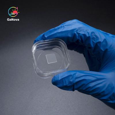
Grado elettronico singolo Crystal Diamond, N Content<100ppb, conducibilità termica di JDCD05-001-003 10*10mm2*0.3mm di XRD<0.015º
Prezzo: Negotiable
MOQ: Negotiable
Tempo di consegna: 3-4 week days
Marca: GaNova
Evidenziare:Electronic Grade Single Crystal Diamond, 10*10mm2*0.3mm Single Crystal Diamond
diamante elettronico di monocristallo del grado di 10*10mm2*0.3mm, tenore di N<100ppb>
PanoramicaI wafer monocristallini del diamante permettono agli avanzamenti critici in entrambi la tecnologia di potere di rf usata per le comunicazioni 5G ed i satelliti; così come nell'elettronica di p... Visualizza di più
Contatta ora

Sistema di ricottura RTP-SA-8
Prezzo: Negotiable
MOQ: Negotiable
Tempo di consegna: 3 month
Marca: Ganova
Evidenziare:Boost Production Rapid Thermal Processing, Rapid Thermal Processing Annealing System
1.Basic configuration of equipment system 1.1outline The Rapid Thermal Processing is a vertical semi-automatic 8-inch wafer rapid annealing furnace, which uses two layers of infrared halogen lamps as heat sources for heating. The internal quartz cavity is insulated and insulated, and the outer shell... Visualizza di più
Contatta ora
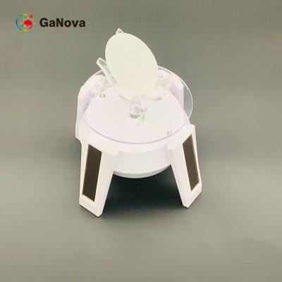
Hall Coefficient Hall Effect Sensor Tester Mobility Resistivity Measurement
Prezzo: Negotiable
MOQ: 1
Tempo di consegna: 8-10week days
Marca: GaNova
Evidenziare:Hall Effect Sensor Tester Mobility Resistivity, carrier concentration hall effect instrument, Hall Effect Sensor Tester semiconductor
Hall Coefficient Hall Effect Sensor Tester mobility resistivity measurement Product Overview: Hall effect tester is used to measure the carrier concentration, mobility, resistivity, Hall coefficient and other important parameters, and these parameters of semiconductor materials to understand the ele... Visualizza di più
Contatta ora
ALN 10*10mm2 AlN singolo cristallo 400±50μM grado S/P/R
Prezzo: Negotiable
MOQ: 1
Tempo di consegna: Negotiable
Marca: GaNova
Evidenziare:ALN aluminum nitride wafer, 2H aluminum nitride wafer, 10*10mm2 aln wafer
AlN substrate is one of the most popular ceramic substrate which has excellent heat resistance, high mechnical strength , abrasion resistance and small dielectric loss . The surface of AlN substrate is quite smooth and low porosity . Aluminium Nitride has higher thermal conductivity , compared to al... Visualizza di più
Contatta ora

94um Laser Diode Chip Slope Efficiency 1.0W/A Wavelength 915nm
Prezzo: Negotiable
MOQ: Negotiable
Tempo di consegna: Negotiable
Marca: GaNova
Evidenziare:94um Laser Diode Chip, high power laser diode chip, 1.0W/A Laser Diode Chip
94μm Laser Diode Chip Slope Efficiency 1.0W/A Wavelength 915nm 915nm 10W COS Diode Laser Chip On Submount Design For low power consumption it is essential that the output from the laser diode (LD) is efficiently coupled to the optical waveguide, and there are several approaches reported in the liter... Visualizza di più
Contatta ora

JDZJ01-001-006 SiC Seed Crystal S Grade 6" Φ153±0,5 mm
Prezzo: Negotiable
MOQ: Negotiable
Tempo di consegna: 3-4 week days
Evidenziare:Cristallo di semi di SiC da 6 pollici, Cristallo di semi di SiC di grado S, φ153±0, 5 mm cristallo di semi di SiC
Sic grado 6" del cristallo di seme S grado φ153±0.5mm di S
Sic può resistere ad una pendenza di tensione (o al campo elettrico) oltre otto volte maggior di che il si o il GaAs senza subire la ripartizione di valanga. Questo campo elettrico di alta ripartizione permette alla lavorazione dei disp... Visualizza di più
Contatta ora
Wafer Ga2O3
(13)
JDCD04-001-002 10x10mm2 (- 201) Sn-ha verniciato la singola Crystal Substrate Product Grade singola lucidatura indipendente di Ga2O3
Prezzo: Negotiable
MOQ: Negotiable
Tempo di consegna: 3-4 week days
Marca: GaNova
Evidenziare:Substrato monocristallino di Ga2O3 in posizione libera, Categoria di prodotto Substrato monocristallino Ga2O3, 10x10mm2 Ga2O3 Substrato monocristallino
10x10mm2 (- 201) Sn-ha verniciato il singolo spessore di lucidatura 0.6~0.8mm FWHM<350arcsec, la resistenza di monocristallo Ga2O3 del substrato del grado indipendente del prodotto di Ra≤0.3 nanometro<9e18>
Dagli anni 90, è stato utilizzato comunemente in diodi luminescenti (LED). Il n... Visualizza di più
Contatta ora
JDCD06-001-005 Wafer di silicio da 6 pollici Dispositivi MEMS Circuiti integrati Substrati dedicati per dispositivi discreti
Prezzo: Negotiable
MOQ: 1
Tempo di consegna: 3-4 week days
Marca: GaNova
Evidenziare:Circuiti integrati Wafer di silicio, Discreti Dispositivi Wafer di silicio, lastra di silicio
dispositivi a 6 pollici della lastra di silicio MEMS, circuiti integrati, substrati dedicati per i dispositivi discreti
Panoramica
Il silicio tipicamente è trovato composto con altri elementi. Gli elementi del silicio possono legare gli atomi strettamente e nelle disposizioni complesse. L'ab... Visualizza di più
Contatta ora
Sapphire Wafer
(19)
C-aereo Sapphire Substrate Wafer di JDCD08-001-006 6inch
Prezzo: Negotiable
MOQ: Negotiable
Tempo di consegna: Negotiable
Evidenziare:6inch Sapphire Substrate Wafer
C-aereo Sapphire Substrate Wafer di JDCD08-001-006 6inch
Gli zaffiri sono in secondo luogo soltanto ai diamanti nella durevolezzaIl diamante è l'elemento naturale più durevole su terra e sulla truppa come i 10 su 10 sulla scala di Mohs di durezza minerale. Gli zaffiri sono inoltre molto durevol... Visualizza di più
Contatta ora

UKAS Patterned Sapphire Substrates Flat Edge Angle
Prezzo: Negotiable
MOQ: 1
Tempo di consegna: Negotiable
Marca: GaNova
Evidenziare:UKAS Patterned Sapphire Substrates, al2o3 substrate 430um, Patterned Sapphire Substrates OEM
50.80±0.10mm Patterned Sapphire Substrates Flat Edge Angle A-Plane±0.2o 2inch Patterned Sapphire Substrates,LED Chip,Substrate Material The efficacy enhancement of GaN-based LEDs with the patterned-sapphire substrate technique is generally attributed to the improvement in both light extraction effic... Visualizza di più
Contatta ora

Supporto per wafer in da 6 pollici per la pulizia di cestini e manici per fiori
Prezzo: Negotiable
MOQ: 1
Tempo di consegna: Negotiable
Evidenziare:6inch Wafer Holder, wafer cassette carrier, 25 PCS Wafer Holder
6inch Wafer Holder Cleaning Flower Baskets And Handles PFA Cassette / Cassette of wafer can be customized and designed by customers’ request, able to resist strong acid, strong hydrofluoric acid, strong base and heat up to 200~220℃, use to deliver wafers in acid & base process of Fabrication f... Visualizza di più
Contatta ora

0.1mm/s To 600mm/s Wafer Dicing Machine X Axis Cutting Range 260mm
Prezzo: Negotiable
MOQ: 1
Tempo di consegna: 8-10week days
Marca: GaNova
Evidenziare:0.1mm/s Wafer Dicing Machine, wafer saw machine 260mm, 600mm/s Wafer Dicing Machine
DAD3350 Wafer Dicing Machine 0.1 ~ 600mm/s X-Axis Cutting Range 260mm Improved throughput The DAD3350 achieves improvement in throughput by increasing the speed of each axis. Ease of use Operability is improved with installation of an LCD touch screen and Graphical User Interface (GUI). Easy operati... Visualizza di più
Contatta ora